Applied Materials Unveils Next-Generation Semiconductor Manufacturing Systems for AI Chips
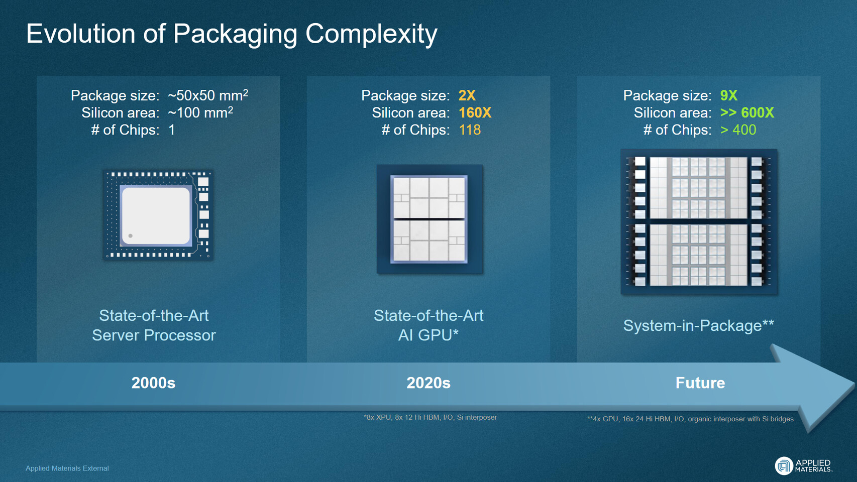
Applied Materials, Inc. has announced a suite of advanced semiconductor manufacturing systems designed to enhance the performance of cutting-edge logic and memory chips, which are essential for artificial intelligence (AI) computing. These new solutions address three pivotal areas in the development of high-performance AI chips: advanced logic technologies such as Gate-All-Around (GAA) transistors, high-performance DRAM including high-bandwidth memory (HBM), and sophisticated packaging methods that enable highly integrated systems-in-a-package. The goal is to optimize chip performance, power efficiency, and cost-effectiveness.
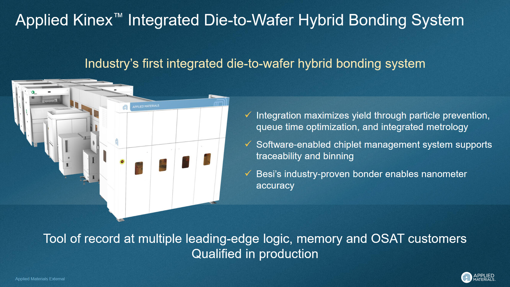
Kinex Bonding System: Advancing Hybrid Bonding for Logic and Memory Chips
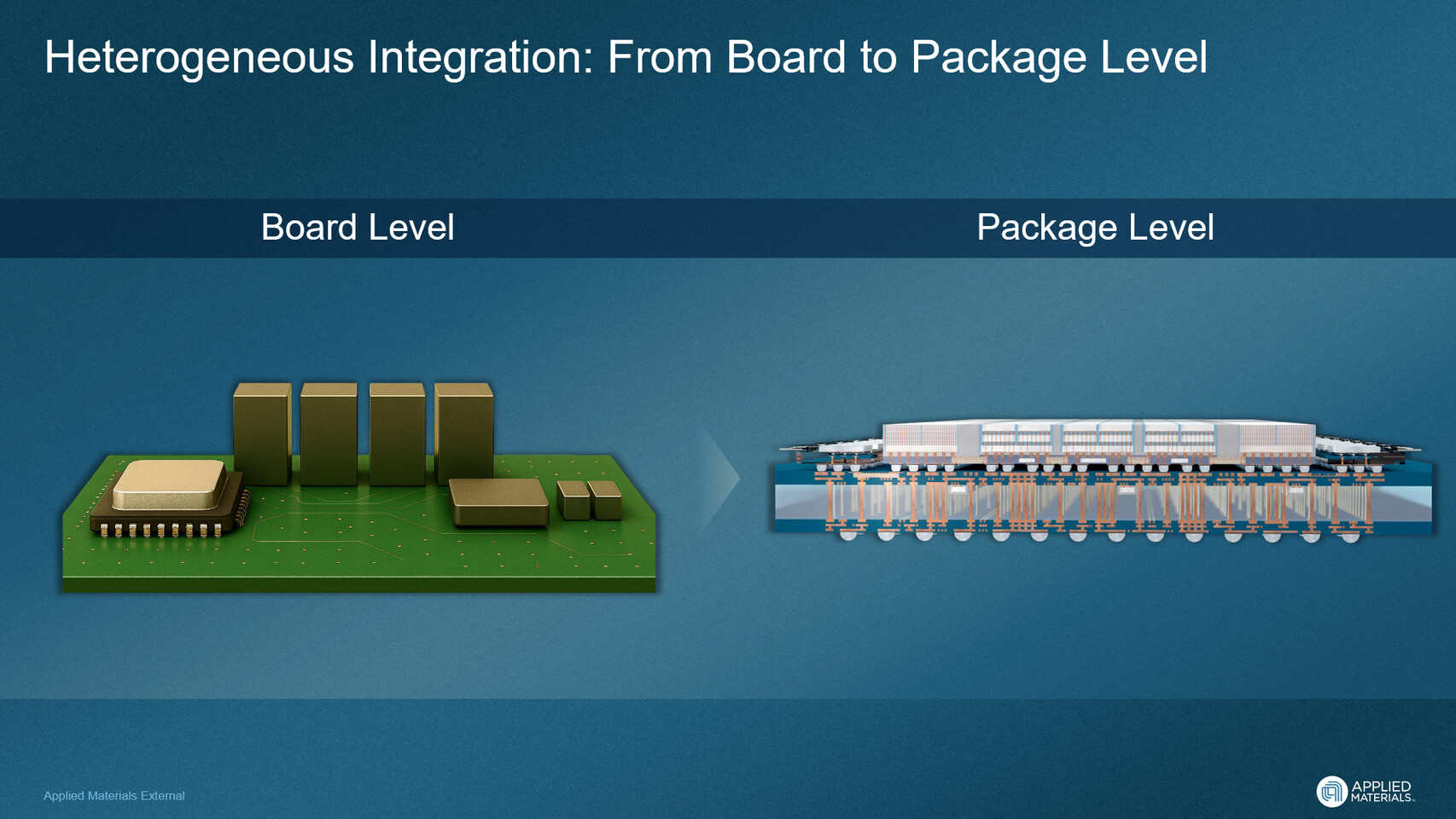
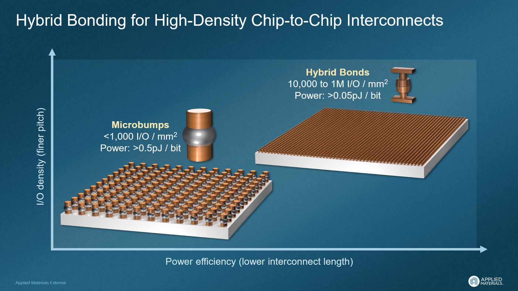
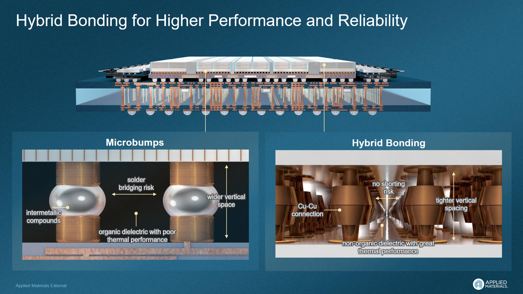
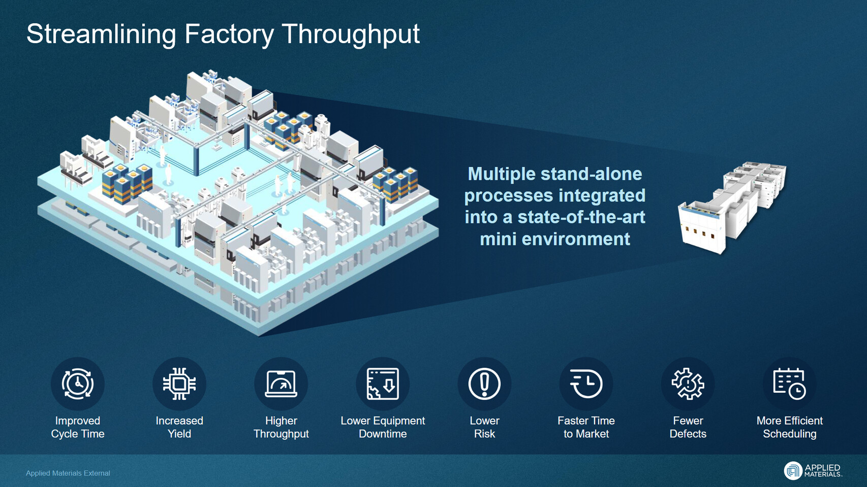
As GPUs and high-performance computing (HPC) chips become more complex, advanced packaging techniques are increasingly used to combine multiple chiplets into intricate systems. Hybrid bonding, a direct copper-to-copper chip-stacking technology, is emerging as a key enabler for improved performance, reduced power consumption, and lower costs.
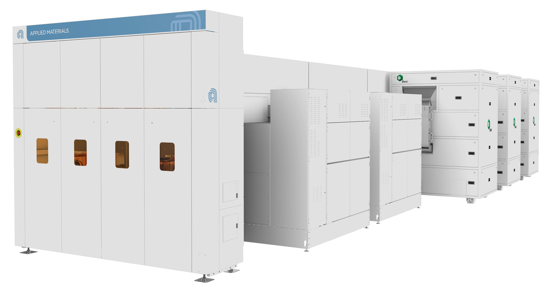
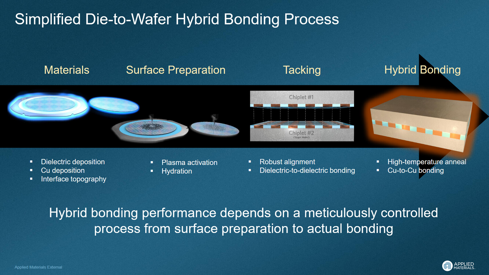
To address the challenges of hybrid bonding in high-volume manufacturing, Applied Materials, in collaboration with BE Semiconductor Industries N.V. (Besi), has developed the Kinex Bonding system—the industry’s first integrated die-to-wafer hybrid bonder. This system merges Applied’s expertise in wafer and chip processing with Besi’s precision die placement and assembly solutions.
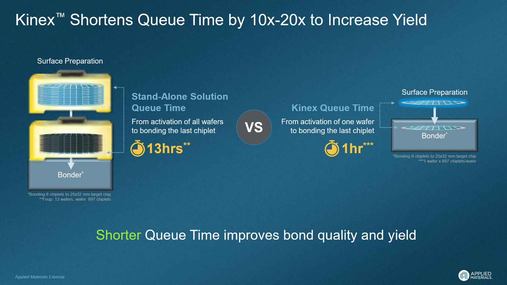
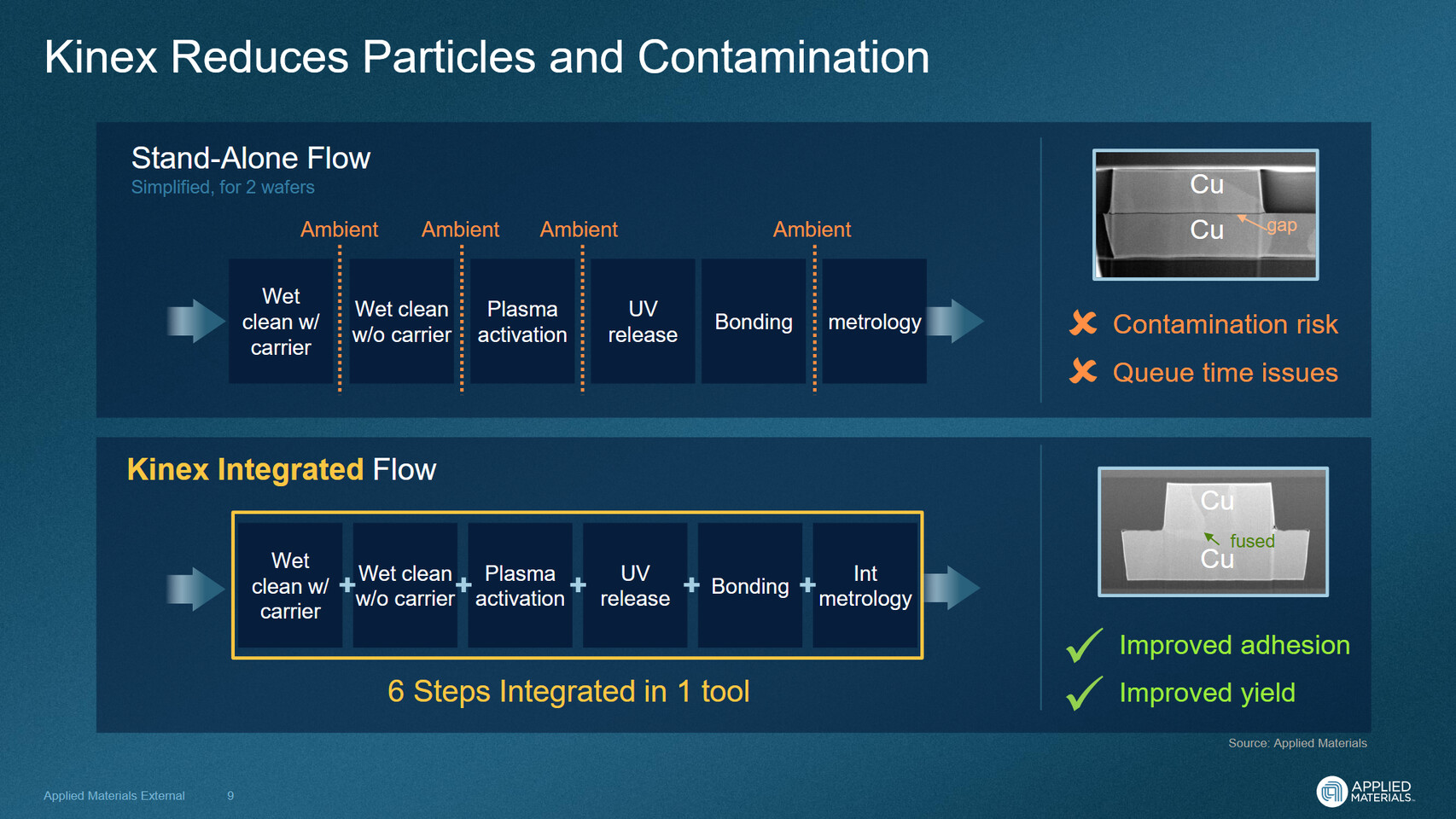
The Kinex system integrates all critical hybrid bonding process steps into a single platform, offering several significant advantages over non-integrated approaches:
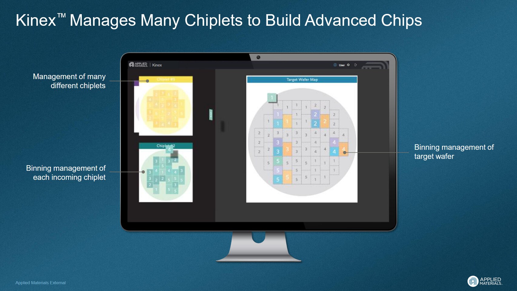
- Enhanced management of complex multi-die packages through superior die-level tracing
- Support for smaller interconnect pitches enabled by high-accuracy bonding in a controlled environment
- Improved bonding consistency and quality via precise control of queue times between process steps
- Faster overlay measurement and drift detection with integrated, in-line metrology
The Kinex Bonding system is already being adopted by leading-edge logic, memory, and outsourced semiconductor assembly and test (OSAT) customers.
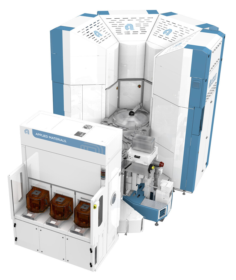
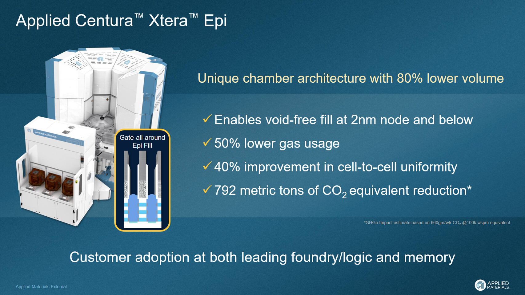
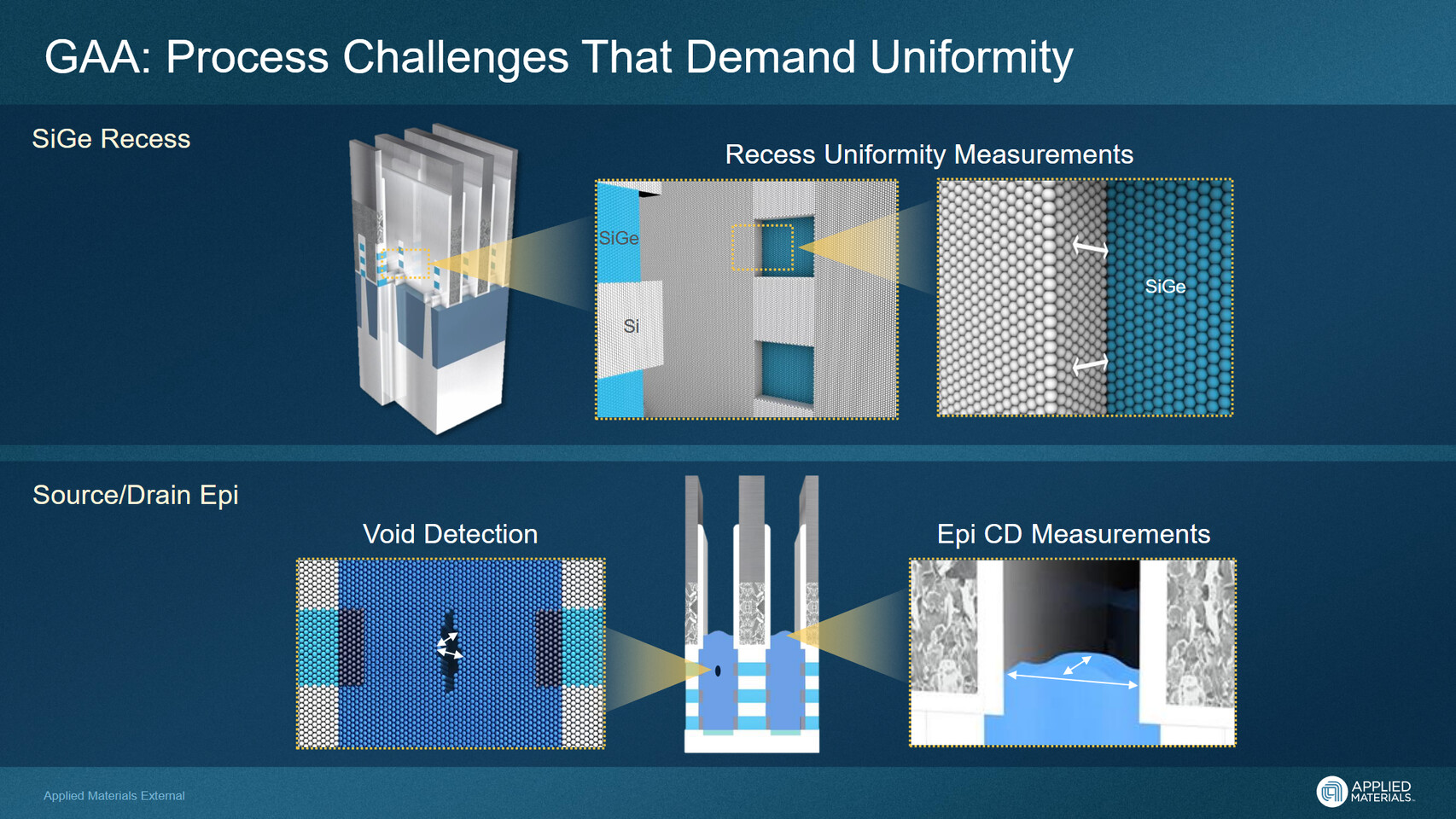
Centura Xtera Epi System: Enabling High-Performance GAA Transistors at 2 nm and Beyond
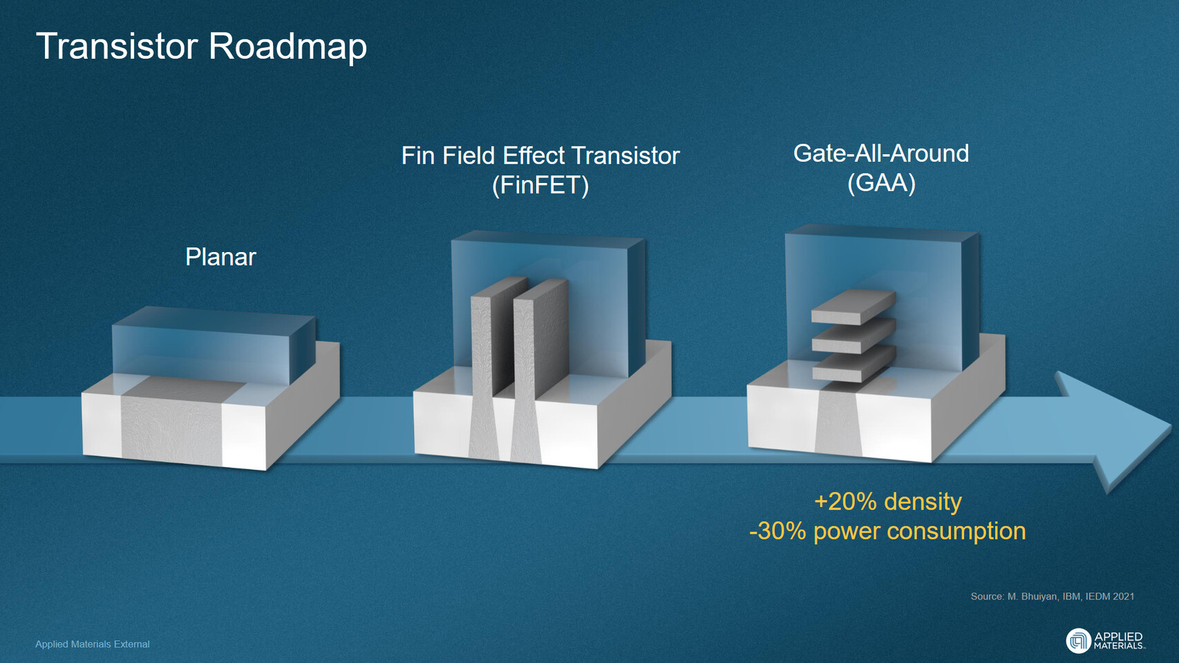
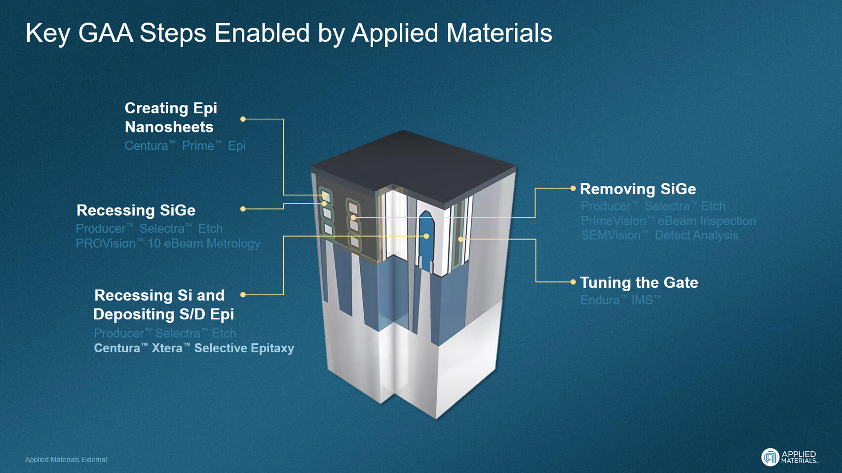
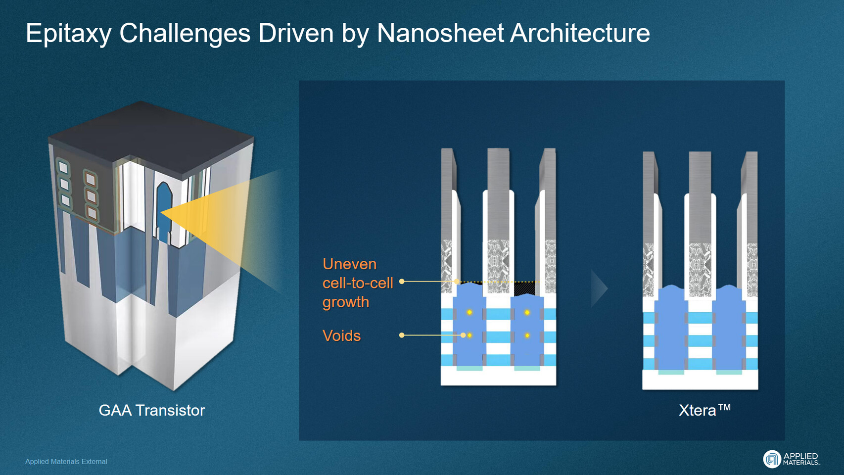
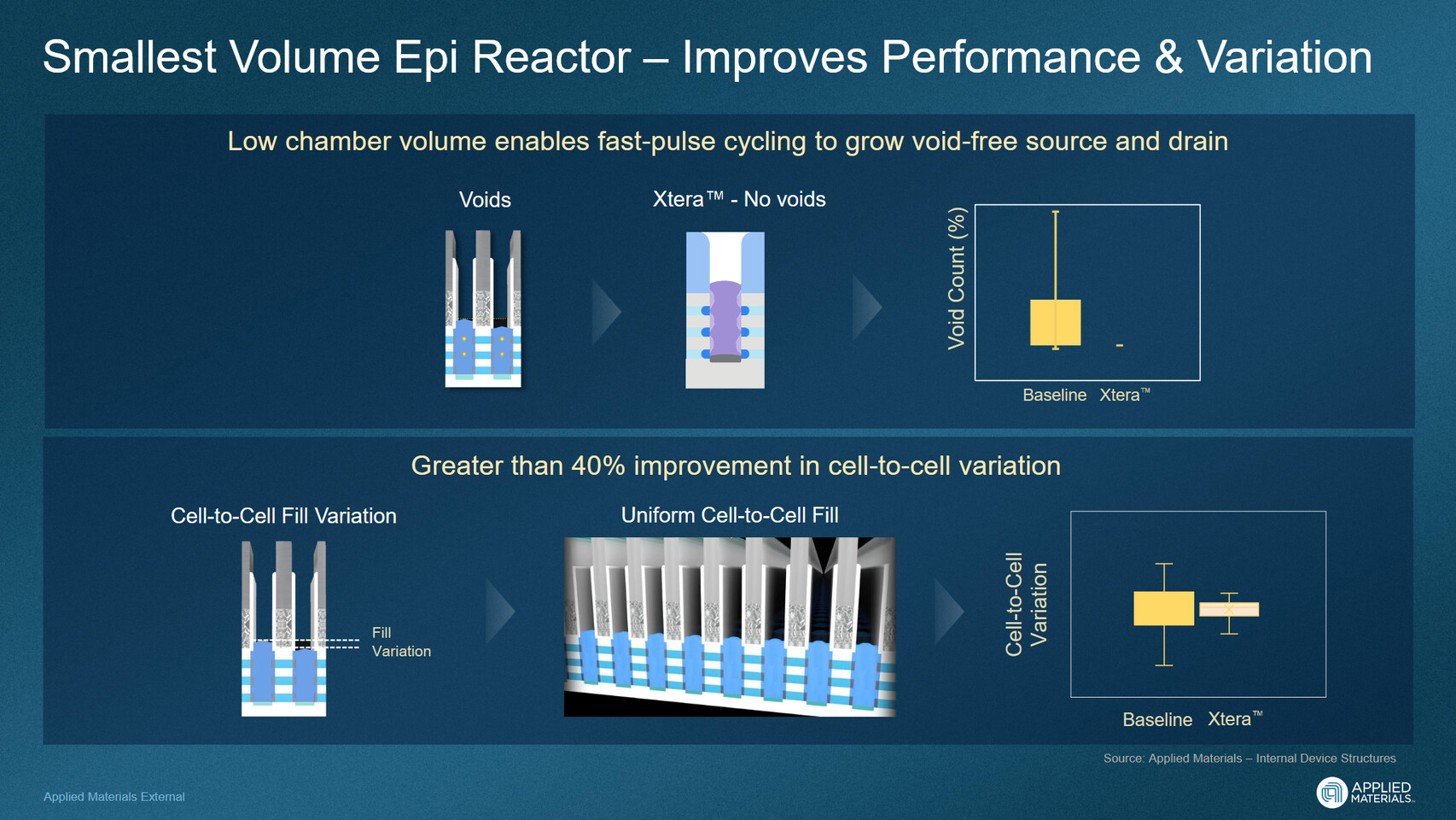
GAA transistors represent a significant advancement in semiconductor technology, with the source and drain structures playing a critical role in device performance and reliability. These structures are formed by depositing materials in deep trenches using an epitaxial (epi) process. However, traditional epi methods can struggle to fill the high aspect ratio trenches of 3D GAA transistors, leading to voids and inconsistent growth that impact performance.
Applied Materials has introduced the Centura Xtera Epi system to address these challenges. Featuring a unique low-volume chamber architecture with integrated pre-clean and etch processes, the Xtera system enables void-free GAA source-drain structures while reducing gas usage by 50% compared to conventional epi. Its innovative deposition-etch process dynamically adjusts the trench opening as material grows, ensuring optimal epi growth across billions of transistors on a wafer. This results in void-free structures and more than 40% improvement in cell-to-cell uniformity.
The Centura Xtera Epi system is being adopted by major logic and memory chip manufacturers to support next-generation device architectures.
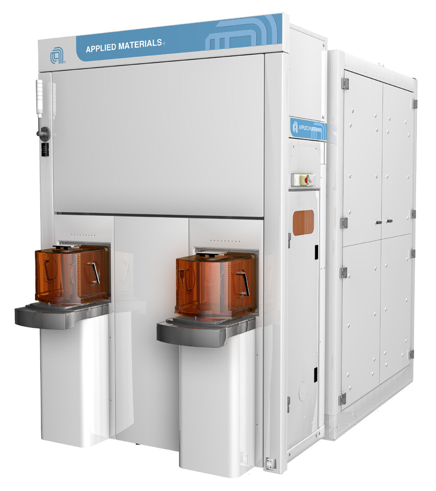
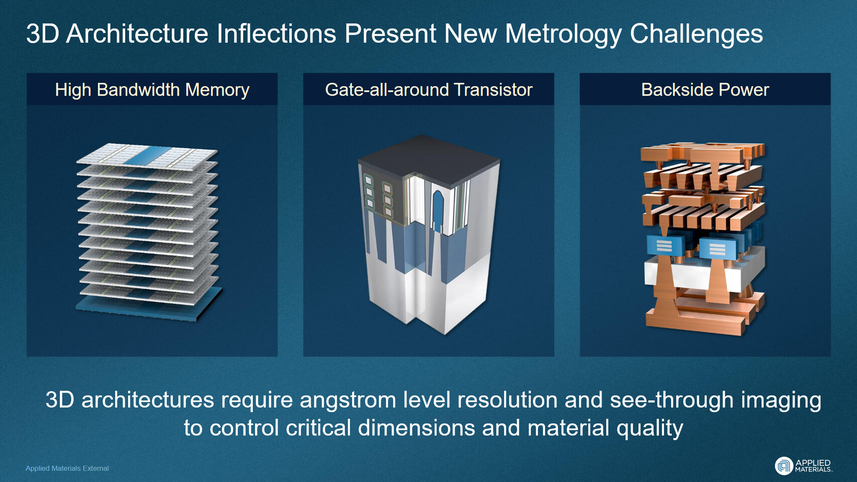
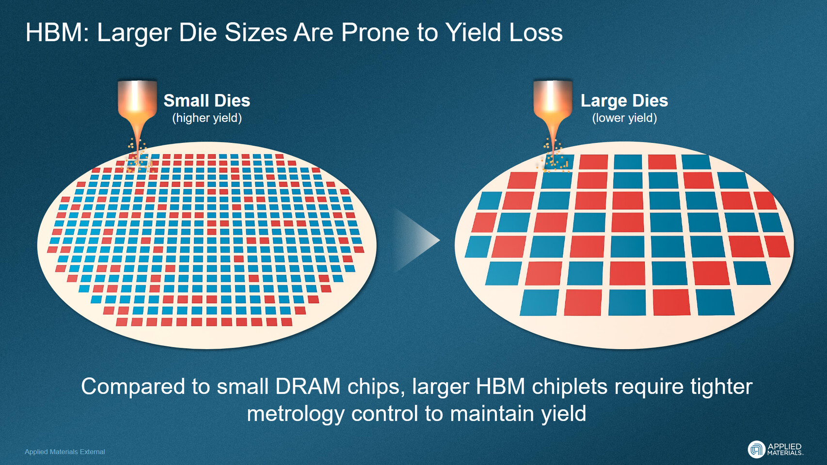
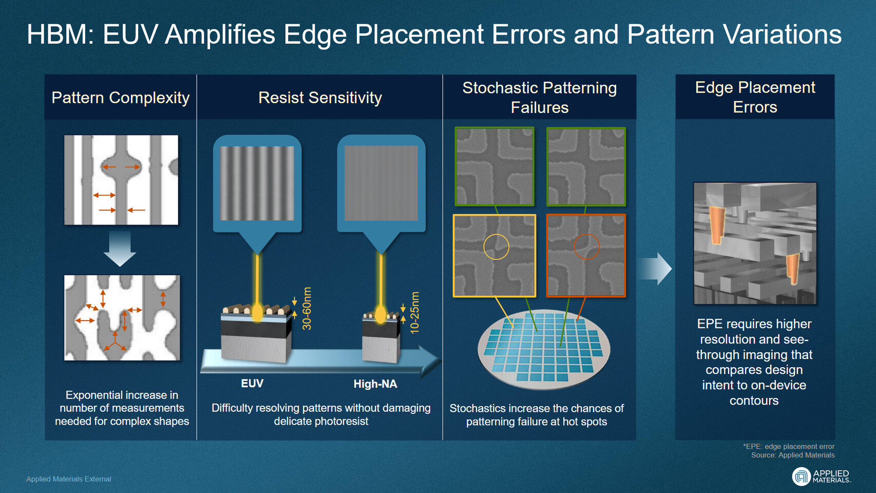
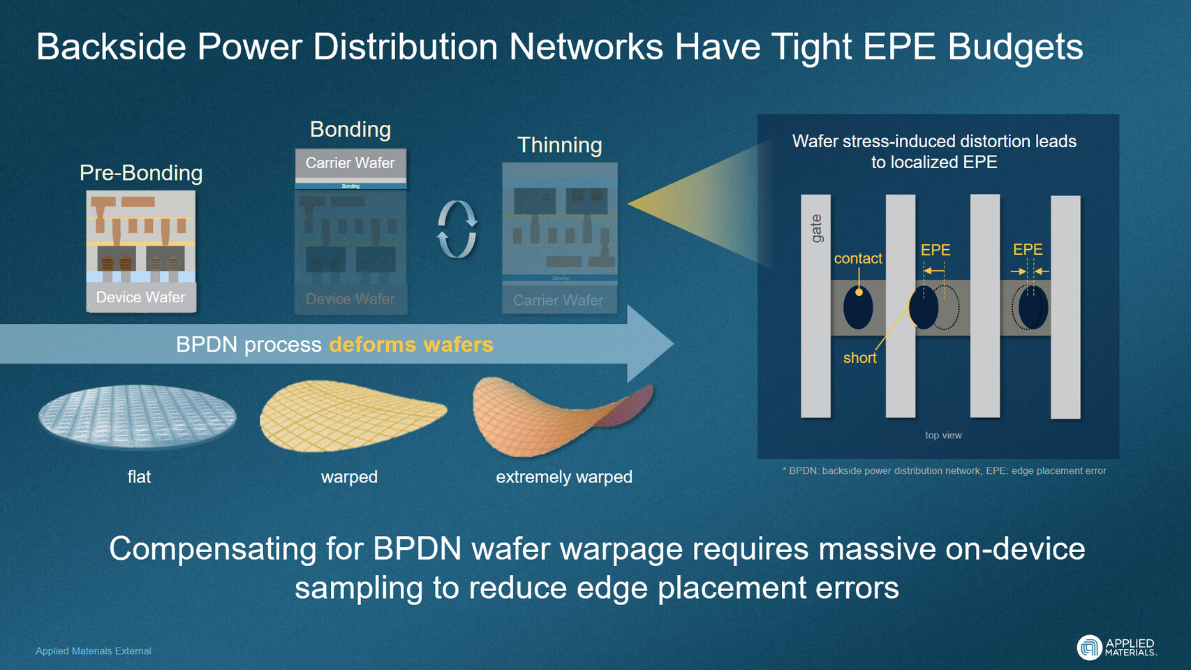
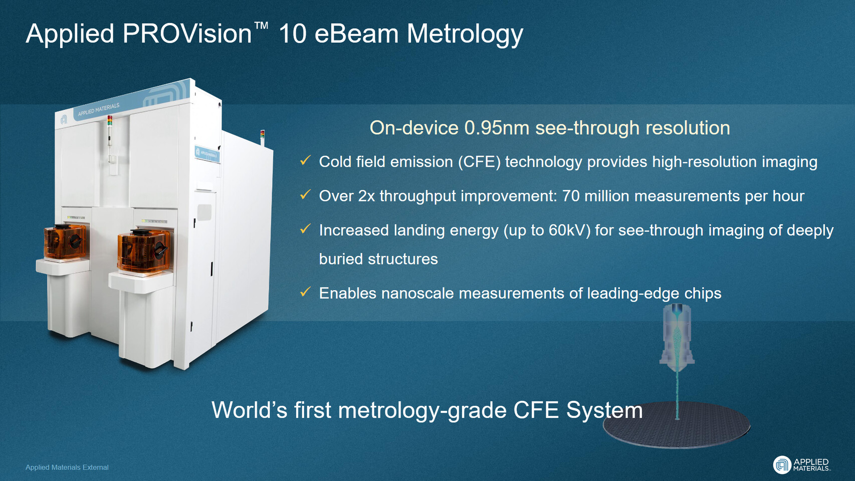
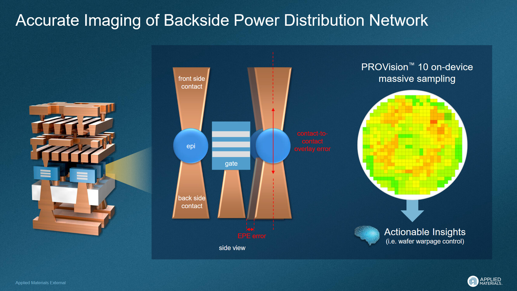
PROVision 10 eBeam Metrology System: Improving Yield for Complex 3D Chips
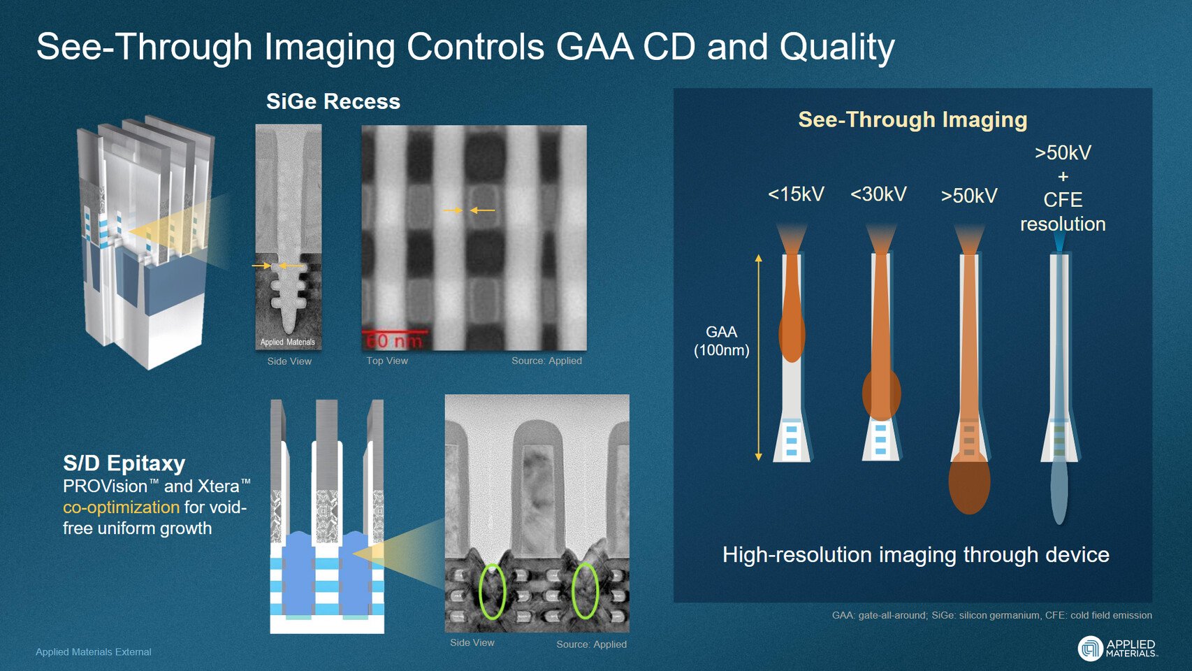
The increasing complexity of 3D architectures in logic and memory chips is pushing the limits of traditional optical metrology. Applied Materials has responded with the PROVision 10, a state-of-the-art eBeam metrology system designed for advanced logic chips—including GAA transistors and Backside Power Delivery architectures—as well as next-generation DRAM and 3D NAND devices.
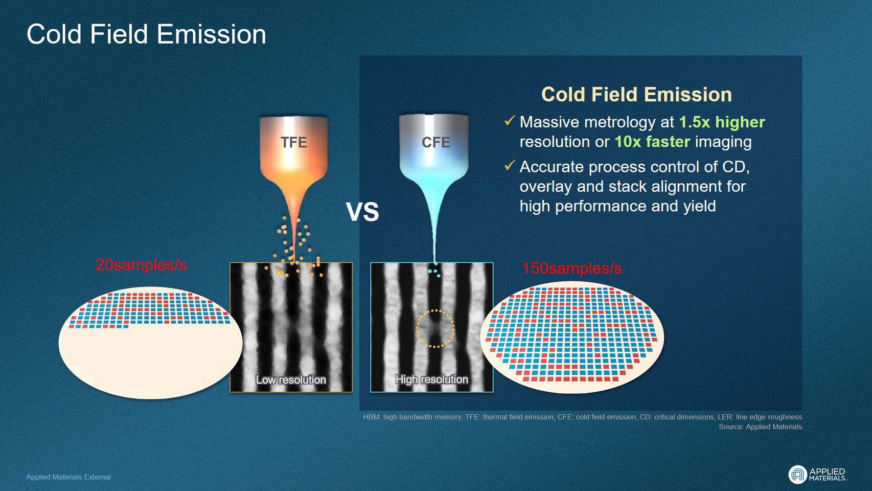
The PROVision 10 is the industry’s first metrology system to incorporate cold field emission (CFE) technology, delivering up to 50% higher nanoscale image resolution and up to 10 times faster imaging speed compared to conventional thermal field emission (TFE) systems. Its sub-nanometer imaging capabilities allow for detailed, multi-layer visualization of 3D chip structures, enabling direct on-device overlay measurements and precise critical dimension (CD) metrology beyond the reach of optical systems.
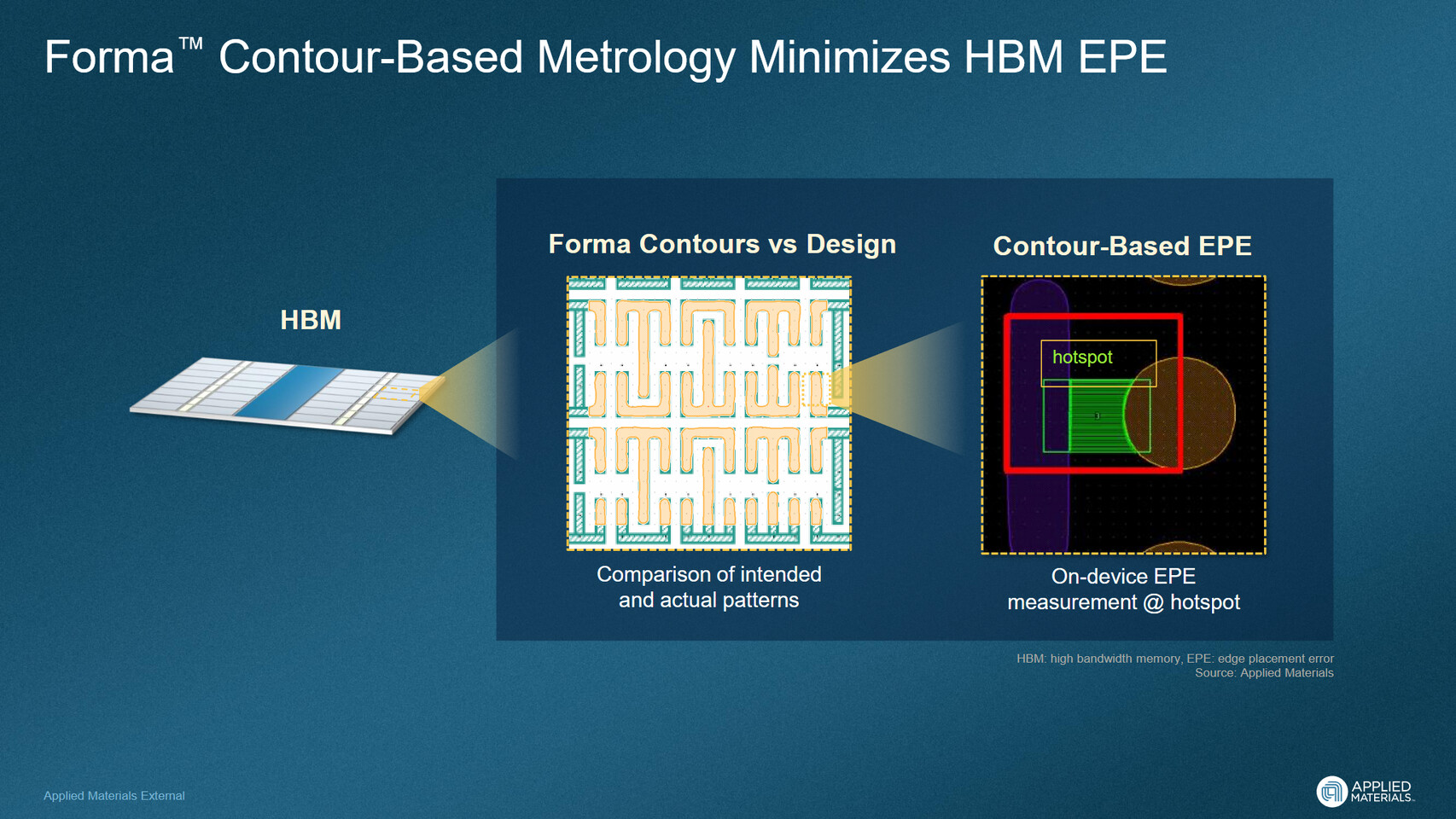
Key process control tasks supported by the PROVision 10 include EUV layer overlay, nanosheet measurement, and epi void detection in GAA transistors. These capabilities make it an essential tool for 2 nm and beyond, as well as for HBM integration. The system is currently in use by several leading logic and memory chipmakers.
With these innovations, Applied Materials is reinforcing its leadership in semiconductor manufacturing technology, supporting the industry’s drive toward more powerful, efficient, and integrated AI chips.