Intel Introduces EMIB-T at ECTC
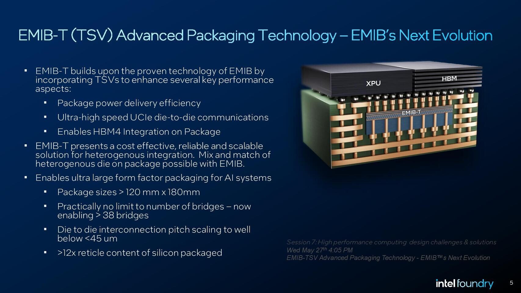
During this week's Electronic Components Technology Conference (ECTC), Intel unveiled EMIB-T, a significant enhancement to its embedded multi-die interconnect bridge packaging. Initially showcased at the Intel Foundry Direct Connect 2025 event, EMIB-T integrates through-silicon vias (TSVs) and high-power metal-insulator-metal capacitors into the existing EMIB structure. Dr. Rahul Manepalli, Intel Fellow and vice president of Substrate Packaging Development, explained that these modifications improve power supply reliability and enhance communication between individual chiplets. Traditional EMIB designs have faced challenges with voltage drops due to their cantilevered power delivery paths. In contrast, EMIB-T directs power through TSVs from the package substrate to each chiplet connection. The integrated capacitors help manage rapid voltage fluctuations and maintain signal integrity.
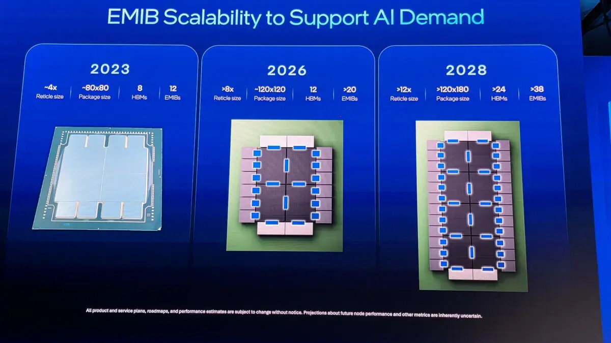
This advancement is crucial for upcoming memory technologies like HBM4 and HBM4e, which are expected to achieve data rates of 32 Gb/s per pin or higher over a UCIe interface. Intel has confirmed that the initial EMIB-T packages will maintain the current energy efficiency level of around 0.25 picojoules per bit while offering increased interconnect density. The company aims to reduce the bump pitch below the current standard of 45 micrometers. Starting in 2026, Intel plans to manufacture EMIB-based packages measuring 120 by 120 millimeters, approximately eight times the size of a single reticle. These large substrates could accommodate up to twelve stacks of high-bandwidth memory and multiple compute chiplets, all interconnected by over twenty EMIB bridges. Looking ahead, Intel envisions expanding package dimensions to 120 by 180 millimeters by 2028, allowing for more than 24 memory stacks, eight compute chiplets, and 38 or more EMIB bridges. These developments align closely with similar strategies announced by TSMC for its CoWoS technology.
In addition to EMIB-T, Intel also introduced a redesigned heat spreader that reduces voids in the thermal interface material by approximately 25%. They also unveiled a new thermal-compression bonding process that minimizes warping in large package substrates.